English
- English

K-S Quality Control
1)PCB Design Rule Check
2)A.O.I testing (Automated optical inspection)
3)E-Test (Electronic test - probe test)
4)X-Ray Testing
- Impedance Control
- Impedance Calculation
- RoHs Lead Free
- PCB Manufacturing tolerances
- PCB UL Certification

OUJINGL ABOUT
关于我们
——
某某家具有限公司出品的一个时尚美式整体家居系列品牌。其英文名GFAFSFAFA源于英文:ASD RFCHN的缩写。为分享惊喜。正如某某图标中的蜂巢中的小蜜蜂。它所传达的正是某某所主张的家居文化:用心经营,分享甜蜜,造就千万个幸福有美好的家,我们的品牌已经传遍了大江南北。大品牌,大信赖。
OUJINGL
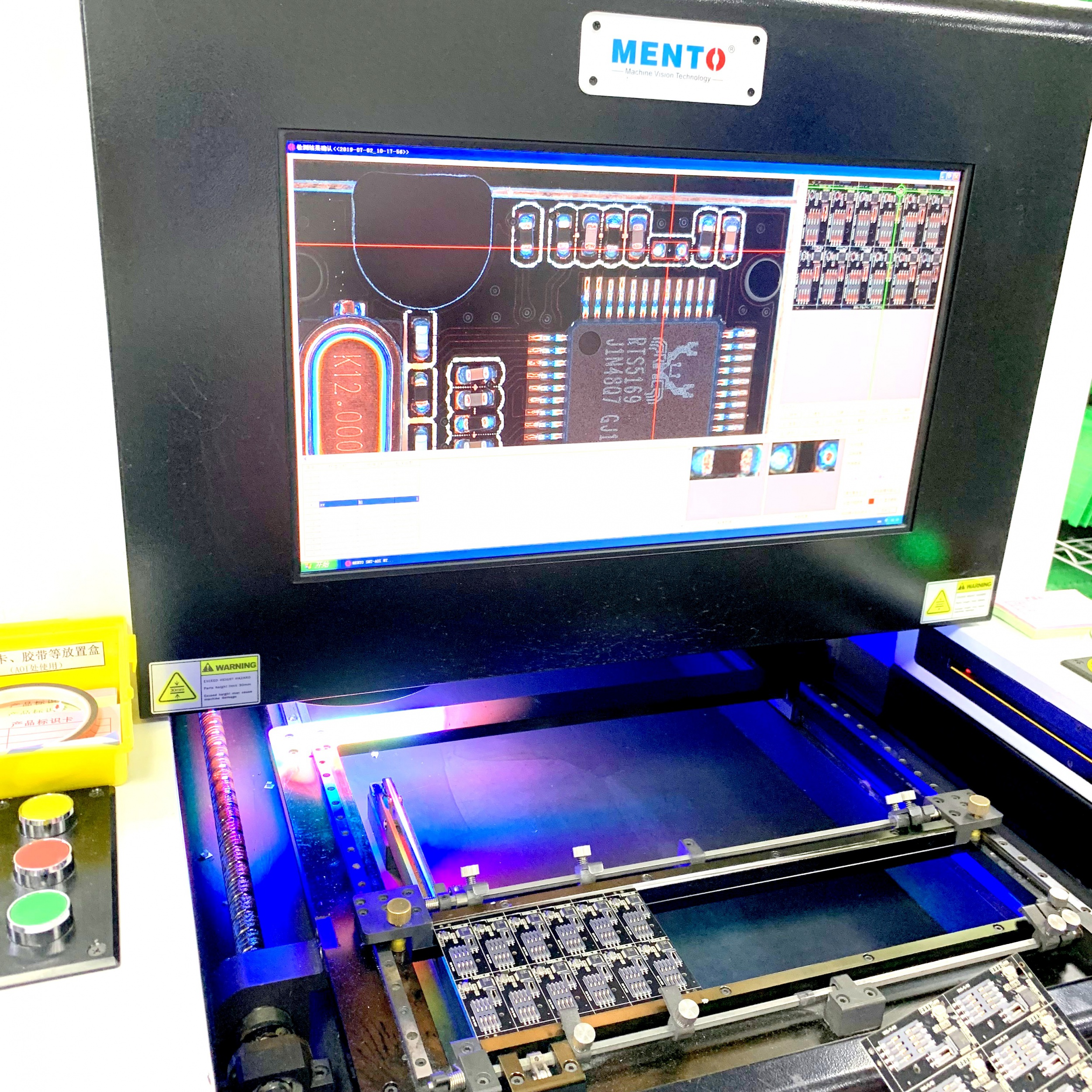
Automated optical inspection (AOI)
The advantage of AOI test
Depending on its visual methods, AOI test can be used to detect a lot of surface defects, such as opens, shorts, incorrect components, missing components etc.
(AOI) is an automated visual inspection of printed circuit board manufacture where a camera autonomously scans the device under test for both catastrophic failure (such as missing component) and quality defects.
It is commonly used in the manufacturing process because it is a non-contact test method. This guarantees the high reliability of Multi-CB multilayer circuit boards.
It is especially important for the following application areas:
- Spacing violation
- Line width violations
- Missing pad
- High frequency
- Short circuits
- High power loads
Electronic test - probe test


The layout is analysed according to the PCB file for short circuits and interruptions.This is important because only the E-test detects incorrect and broken conductors. And the detected defective circuit board will be rejected or marked.

Combine Automatic optical alignment system and the traditional flying needle machine together,with the help of image-processing software and flying-pin-only cameras, flying probe test is easier and more accurate.

Each production batch of a circuit board is a one-time process, and the E-Test has to be conducted each time
Automated X-Ray Inspection
X-ray inspection systems are able to monitor a variety of aspects of a printed circuit board assembly production. It can not only check the solder joints that are under packages such as BGAs, CSPs and flip chips where the solder joints are hidden but also reveal many defects in solder joints that may not be visible with ordinary optical inspection equipment. They would normally be placed after the solder process to monitor defects in PCBs after leaving the soldering process.


CONTACT
Contacts:Kelly
E-mall:info@k-selectronics.com
Address:215, Building A,Lian Gao, No.8230 Bao'an Avenue, Xinqiao Street, Bao'an District, Shenzhen Republic of China, Postal Code 518125
Website:www.k-selectronics.com
©2019 K-S ELECTRONICS All Rights Reserved
Record Number: 粤ICP备12345678号 Sitemap
©2019 K-S ELECTRONICS有限公司 版权所有
